Designing a complex PCB isn't just about connecting dots; it's about engineering a robust, high-performance system that works flawlessly the first time. For those ready to push past basic schematics and simple two-layer boards, mastering Advanced KiCad Workflows becomes essential. It’s the difference between a prototype that barely functions and a manufacturable product ready for the real world, especially when dealing with high-speed signals, multi-layer stackups, and compact IoT devices like an ESP32.
If you’ve moved beyond KiCad’s foundational features and are tackling projects that demand precision, signal integrity, and manufacturability, you know the stakes are higher. This guide is your deep dive into the sophisticated techniques and thoughtful strategies that seasoned engineers employ to bring advanced designs to life using KiCad.
At a Glance: What You'll Master in Advanced KiCad Workflows
- Strategic Project Setup: Efficiently organizing complex designs with hierarchical schematics and robust libraries.
- Optimized Component Placement: Balancing performance, thermal management, and manufacturability.
- High-Speed Signal Integrity: Routing critical paths like SPI, I²C, and USB with controlled impedance and noise reduction.
- Multi-Layer Stackups: Designing effective power and ground planes for stability and EMC.
- Rigorous Design Checks: Implementing advanced DRC and DFM for flawless production.
- Iterative Design & Troubleshooting: Learning from prototypes and refining designs for optimal performance.
- Manufacturing Readiness: Generating precise fabrication files and documentation.
Beyond the Basics: Why Advanced KiCad is Your Next Frontier
You've successfully designed a few PCBs. You understand how to draw a schematic, lay out traces, and maybe even generate Gerbers. But what happens when your project scales up? When you need an ESP32-based IoT device with multiple sensors, SD card storage, flash memory, and USB-C connectivity, all packed onto a four-layer board? That's where basic KiCad knowledge hits its limits, and advanced workflows become your superpower.
These advanced techniques aren't just about using more features; they're about adopting a methodical, engineering-driven approach. It’s about anticipating problems before they happen, ensuring signal integrity on a high-speed bus, and designing for thermal performance, all while keeping manufacturing costs and reliability in mind. You’re not just drawing; you’re architecting.
Building Your Foundation: Strategic Project Setup for Complexity
The secret to managing complex designs in KiCad starts before you even draw your first wire. A well-structured project setup saves countless hours and prevents headaches down the line.
Hierarchical Schematics: Conquering Complexity, One Sheet at a Time
Imagine trying to cram an entire ESP32 IoT system – microcontroller, power management, multiple sensors, memory, and USB — onto a single schematic sheet. It would be an unreadable mess. Hierarchical schematics are your antidote.
This powerful feature allows you to break down your design into logical, manageable blocks. Each block, like "Power Supply," "ESP32 Core," or "Sensor Array," gets its own dedicated sheet. These sheets connect through global labels or hierarchical pins, creating a clear, modular structure that's easy to navigate, debug, and reuse. For a robust multi-layer ESP32 project, this isn't just a convenience; it's a necessity. It’s a key step in learning how to master hierarchical schematic design efficiently.
Mastering Your Libraries: Custom Components and 3D Models
While KiCad offers extensive default libraries, advanced designs often require custom components, unique footprints, or specific 3D models for accurate visualization and mechanical checks. Relying solely on default libraries can lead to compromises or, worse, errors in manufacturing.
- Creating Custom Symbols and Footprints: Learn to build precise symbols and footprints from datasheets. Pay close attention to pad sizes, clearances, and silkscreen for optimal assembly. For instance, ensuring your USB-C connector footprint has robust pads and proper clearances for manufacturability is paramount.
- Integrating 3D Models: Attaching 3D models to your footprints provides invaluable visual verification. It helps identify potential mechanical clashes early in the design phase, especially when dealing with enclosures or tightly packed components like an SD card module or flash memory alongside an ESP32. This also ties into creating custom component footprints that include proper 3D representations.
- Library Management: Develop a systematic approach to managing your custom libraries. Store them in a version-controlled environment and clearly name your assets. This ensures consistency across projects and makes collaboration smoother.
The Blueprint for Performance: Advanced Schematic Capture
With your project structure in place, the actual schematic drawing moves into an advanced realm where signal integrity and component interaction take center stage.
Beyond Basic Connections: Signal Integrity at the Schematic Level
A schematic isn't just a netlist; it's the foundation of your board's electrical performance. Advanced designers consider signal integrity from the very beginning.
- Decoupling Capacitors: Understand why and where to place decoupling capacitors. Near the power pins of your ESP32, flash memory, and other ICs, these aren't optional – they're critical for stable power delivery, especially during high-speed switching. The course on designing an ESP32 IoT board emphasizes this, especially for sensitive components.
- Grounding Strategies: Plan your grounding hierarchy. How will different ground domains connect? How will you isolate noisy analog signals from digital? Even at the schematic level, clear ground net definitions help guide your PCB layout.
- Component Selection for Performance: Choose components not just for function, but for their electrical characteristics. For instance, selecting the right type and value of capacitors for sensor filtering (like a photosensor) directly impacts performance. The redesign phase of the ESP32 course specifically highlighted correcting photosensor wiring with proper capacitor placement, underscoring this importance.
Precision in Placement: Optimizing for Manufacturability and Performance
Once your schematic is complete, the physical layout begins. Advanced placement isn't just about fitting components; it's about strategic positioning for optimal electrical performance, thermal management, and ease of manufacturing.
The Art of Component Grouping and Orientation
Think of your PCB as a tiny city. Group related components together (e.g., ESP32, flash, and critical decoupling capacitors; USB-to-serial bridge with its connectors and support components). This minimizes trace lengths, reduces noise, and makes routing more intuitive.
- Thermal Considerations: Components like the ESP32 can generate heat. Plan for thermal dissipation by placing heat-sensitive components away from major heat sources or by designing in thermal vias and large copper pours. This is vital for optimizing PCB thermal management.
- Manufacturability (DFM):
- Keepout Areas: Define clear keepout zones for mechanical components (enclosures, mounting hardware) and specific electrical considerations (RF antennas).
- Test Points: Strategically place test points for debugging and post-manufacturing testing.
- Component Accessibility: Ensure buttons, connectors (like your USB-C), and indicators are easily accessible and properly spaced. The ESP32 redesign examples from the course specifically mention enlarging buttons and refining their placement, highlighting the practical impact of DFM considerations.
- Refining Placement Iteratively: Don't expect perfect placement on the first try. An uncut layout video of an ESP32 design in KiCad 9 revealed the iterative nature of placement – moving components, adjusting orientations, and making decisions in real-time based on routing challenges and DFM considerations. Embrace this process.
Navigating the Nerves: High-Speed Routing Masterclass
Routing high-speed signals is where advanced KiCad truly shines. Incorrect routing can lead to signal degradation, EMI issues, and an unstable board.
Controlled Impedance Routing: Taming High-Speed Buses
For interfaces like SPI, I²C, and especially USB, maintaining controlled impedance is paramount. KiCad allows you to define trace widths and clearances to achieve a target impedance, critical for minimizing reflections and ensuring reliable data transfer.
- Differential Pairs: USB, for example, uses differential pairs. KiCad's differential pair routing tool ensures both traces are routed in parallel, maintain consistent spacing, and have matched lengths, which is crucial for noise immunity and signal integrity.
- Length Matching: For parallel buses or clock-data pairs, ensuring traces have similar lengths prevents skew. KiCad’s length-tuning tools let you add serpentine traces to precisely match lengths.
- Via Stitching and Ground Pours: Use plenty of ground vias to stitch ground planes together, creating a solid return path for high-speed signals. This minimizes ground bounce and improves EMI performance.
Noise Reduction Techniques: Ferrite Beads and Filtering
Beyond just routing, advanced designs incorporate specific components to combat noise.
- Ferrite Beads: These components act as frequency-dependent resistors, effectively choking high-frequency noise on power lines or signal paths without significantly impacting DC current. The ESP32 redesign added a ferrite bead for noise reduction, a clear indicator of its importance in complex, sensitive designs.
- Proper Capacitor Placement: While mentioned in schematics, placement on the PCB is critical. Capacitors for filtering or decoupling must be placed as close as possible to the component they protect to be effective. The photosensor wiring correction in the ESP32 redesign, involving precise capacitor placement, illustrates this perfectly. These are all part of advanced high-speed routing techniques.
- Refining Track Routing: Don't just auto-route and call it a day. Manually review and refine critical tracks. Ensure smooth curves, avoid sharp 90-degree bends (which can cause impedance discontinuities), and maintain adequate spacing between signals to prevent crosstalk.
Power and Ground Planes: The Unsung Heroes
For a multi-layer board, copper zones and intelligent stackup design provide robust power delivery, stable grounding, and excellent thermal performance.
Multi-Layer Stackup Design: More Than Just Layers
A four-layer board, as used in the ESP32 IoT project, typically follows a specific stackup: Signal-Ground-Power-Signal. This arrangement provides:
- Excellent Ground Reference: A solid ground plane beneath your signal layers provides a clear, low-impedance return path for signals, crucial for high-speed operation and EMI reduction.
- Stable Power Delivery: A dedicated power plane offers a low-inductance source for all components, minimizing voltage ripple.
- EMI Shielding: Internal ground and power planes act as shields, containing electromagnetic radiation within the board.
Copper Zones for Power Distribution and Thermal Management
Copper zones (also known as pours or polygons) are fundamental.
- Power Distribution: Instead of routing individual power traces everywhere, use large copper zones for VCC, 3.3V, 5V, and ground. This provides a much lower impedance path, reducing voltage drops and improving power integrity.
- Thermal Management: Large copper zones on surface layers (or internal layers connected by thermal vias) act as heatsinks, efficiently drawing heat away from components like the ESP32 and dissipating it across the board. This directly impacts long-term reliability.
- Split Planes vs. Solid Planes: While solid ground planes are generally preferred for high-speed digital, sometimes split planes are necessary for mixed-signal designs to isolate analog and digital grounds. Understand the trade-offs and design accordingly to prevent noise coupling.
The Iron Check: DRC and DFM for Flawless Boards
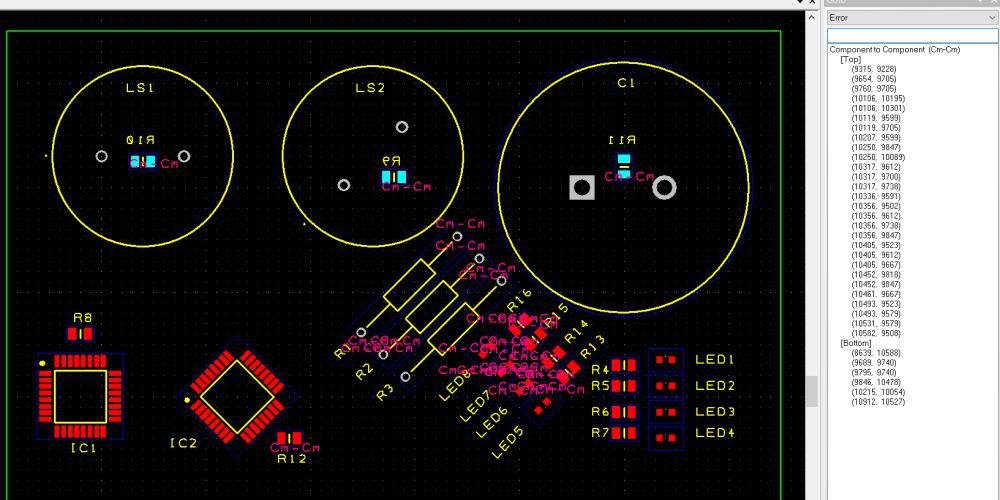
Even the most meticulously designed board can have subtle errors. This is where KiCad's robust Design Rules Check (DRC) and your understanding of Design for Manufacturing (DFM) become indispensable.
Advanced DRC: Custom Rulesets and Error Resolution
KiCad’s DRC isn’t just for basic clearances. You can define highly specific rules:
- Minimum Trace Widths: Enforce minimum widths for power lines or high-current paths.
- Via Rules: Specify minimum via diameters and annular ring sizes.
- Differential Pair Rules: Ensure correct spacing and length tolerances for high-speed pairs.
- Net Class Rules: Apply different rules to different net classes (e.g., high-voltage nets might need wider clearances).
The key is not just running DRC, but systematically understanding and resolving every reported error and warning. Sometimes, a warning might be acceptable, but never ignore one without understanding its implication. This is a core element of best practices for DFM and DRC.
Design for Manufacturing (DFM) Analysis: Thinking Like a Manufacturer
DFM goes beyond DRC, considering how your board will actually be fabricated and assembled.
- Panelization: For small boards, how will your manufacturer panelize them to optimize cost? Design with proper breakaway tabs and fiducials in mind.
- Solder Mask and Paste Mask: Ensure adequate solder mask clearances and appropriate paste mask apertures for reliable soldering, especially for fine-pitch components.
- Component Spacing: Leave enough room between components for pick-and-place machines and for hand soldering/rework if needed.
- Fiducial Marks: Include global and local fiducial marks for automated assembly machines.
The iterative design process of the ESP32 course, which included a redesign to fix issues from a first prototype, is a testament to the importance of DFM. Learning from prototype #1 led to practical improvements like enlarging buttons, track routing refinements, and proper capacitor placements, all driven by real-world evaluation.
From Concept to Coded Reality: Post-Design & Evaluation
Your design is complete, DRC/DFM checks are passed. Now, it’s time to prepare for manufacturing and get ready to test your creation.
Generating Fabrication Files: The Language of Manufacturers
KiCad generates all the necessary files your PCB manufacturer needs:
- Gerber Files: These are standard files (RS-274X format) for each copper layer, solder mask, silkscreen, and paste mask. Double-check that all layers are exported correctly.
- Drill Files: A separate file (Excellon format) detailing all drill holes.
- Netlist: Often used by manufacturers for electrical testing.
- Board Outline: A clear outline of your PCB’s dimensions.
Always use a Gerber viewer to inspect your generated files before sending them off. This final visual check can catch unexpected issues.
Bill of Materials (BOM) and Centroid Files: For Assembly
These are crucial for automated assembly:
- Bill of Materials (BOM): A comprehensive list of all components, including part numbers, quantities, and descriptions. KiCad can generate this directly from your schematic.
- Centroid File (Pick-and-Place File): This file lists the X/Y coordinates, rotation, and layer for each surface-mount component, guiding the automated pick-and-place machines.
Board Evaluation and Troubleshooting: The Acid Test
Once your boards arrive, the real fun begins: testing.
- Firmware Integration: For an ESP32 board, loading initial Arduino firmware is often the first step to test basic functionality (LEDs, serial communication).
- Systematic Testing: Test each functional block methodically. Does the power supply provide correct voltages? Do the sensors respond? Is the USB-to-serial bridge working?
- Debugging: Use multimeters, oscilloscopes, and logic analyzers to pinpoint issues. Understanding the expected signals and voltages from your schematic is critical here. The course specifically includes post-manufacturing board evaluation and troubleshooting using Arduino firmware, underscoring this crucial phase.
- Learning from Prototypes: The most advanced engineers embrace failure as a learning opportunity. The ESP32 project’s course updates explicitly detail a redesign based on issues found in the first prototype. This iterative approach is key: identifying audio and light sensor wiring issues, integrating a variable resistor for adjustable audio gain, correcting photosensor wiring, and making layout refinements all stem from rigorous evaluation.
When Things Go Sideways: Learning from Prototypes (ESP32 Case Study)
The journey to a perfect PCB is rarely linear. Advanced designers recognize that prototypes are for learning, not just validation. The "KiCad Advanced ESP32 Project" provides an excellent real-world example of this iterative process, highlighting typical issues and their solutions:
- Sensor Input Correction: Initial designs for audio and light sensors might use inappropriate ADC pins or lack proper filtering. The redesign moved these to ADC1 and ensured correct capacitor placement, demonstrating how a small change can significantly impact analog performance.
- Adjustable Gain for Audio: To enhance functionality, a variable resistor was integrated into the audio amplifier circuit. This shows a design refinement based on desired operational flexibility, adding a new layer of complexity to manage in layout.
- Photosensor Capacitor Placement: A seemingly minor detail, the precise placement of a capacitor for the photosensor can drastically improve its stability and noise immunity. This highlights the importance of localized filtering.
- Mechanical and Routing Refinements:
- Enlarging Buttons: A common DFM issue; buttons that are too small or too close together are difficult to use. Enlarging them improves user experience and manufacturability.
- Refining Track Routing: Continuous review of trace paths to reduce noise, shorten critical paths, and optimize for manufacturability, even after an initial pass.
- Ferrite Bead Addition: Proactively adding a ferrite bead to a power or signal line to mitigate noise, a solution born from observing real-world prototype behavior.
- Updating Footprints and 3D Models: As designs evolve, components might change, or better models become available. Keeping your libraries updated ensures consistency and accuracy.
Embracing these redesign cycles and documenting the "fixes and decisions" – as shown in the uncut layout video – is the hallmark of an advanced workflow. It transforms issues into insights, leading to a truly robust final product. For deeper dives into component specifics and their impact on design, you can always Learn more about KiCad software and its evolving capabilities.
Your Next Steps in Advanced KiCad
Mastering advanced KiCad workflows isn't about memorizing features; it's about adopting an engineering mindset. It's about thinking critically about signal paths, power delivery, thermal management, and manufacturability at every stage of the design process.
If you’re ready to build complex, high-performance PCBs with confidence, practice is key. Start with a multi-layer design, experiment with high-speed routing, and meticulously review your DRC and DFM outputs. Don't be afraid to iterate; every prototype, whether successful or not, offers invaluable lessons.
For those looking to accelerate their journey, consider structured learning paths. Resources like the "KiCad Advanced ESP32 Project" are specifically designed to guide you through these intricate processes, using real-world projects like a four-layer ESP32 IoT PCB as your training ground. You’ll be designing robust, high-speed boards that not only work, but impress.