Imagine transforming your electronic ideas into tangible circuits without the burden of expensive software licenses. KiCad makes this a reality. This free and open-source Electronic Design Automation (EDA) suite empowers hobbyists, students, engineers, and startups alike to design professional-grade Printed Circuit Boards (PCBs) from concept to fabrication, all without cost or restriction. It's a complete ecosystem for innovation, running seamlessly across Windows, macOS, and Linux.
KiCad isn't just "free"; it's a powerful, community-driven tool that rivals proprietary solutions, constantly evolving with significant contributions from institutions like CERN. Whether you're building a simple blinking LED circuit or a complex multi-layer motherboard, KiCad provides all the features you need. This comprehensive guide will navigate you through its capabilities, helping you unlock your full design potential.
Unlocking Professional PCB Design Accessibility
At its core, KiCad democratizes PCB design. Traditionally, high-quality EDA tools came with hefty price tags, creating a barrier to entry for many. KiCad shatters this barrier, offering a full suite of tools for schematic capture, PCB layout, 3D visualization, and even circuit simulation – all completely free and open-source. This means anyone, anywhere, can download it and start designing immediately.
The freedom from licenses, usage limits, or hidden restrictions fosters an environment of experimentation and innovation. It's an ideal platform for educational institutions, open-source hardware projects, and even small businesses looking to keep development costs low without compromising on professional output. Ready to dive in? Our guide on how to Get started with KiCad will walk you through the installation and initial setup.
From Concept to Circuit: The KiCad Design Workflow
The journey of creating a PCB begins with an idea, which then translates into a schematic, and finally into a physical layout. KiCad provides distinct, yet integrated, tools for each stage of this process, allowing for a flexible and powerful workflow.
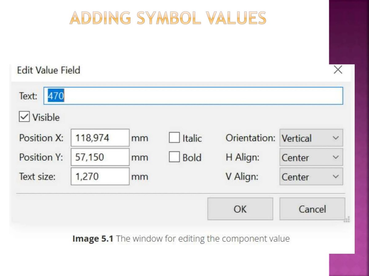
Crafting Your Vision with the Schematic Editor
The schematic is the blueprint of your electronic circuit, where you logically connect components. KiCad's Schematic Editor is incredibly robust, supporting designs from basic circuits to complex hierarchical projects spanning hundreds of sheets. You can utilize thousands of components from the official KiCad library or create your own custom symbols, ensuring every unique part of your design is accurately represented.
Beyond just drawing connections, the schematic editor includes an integrated SPICE simulator for analog circuit analysis and an Electrical Rules Checker (ERC) to catch common design errors early on. Understanding how to organize your components and connections effectively is crucial. To master this foundational step, explore our KiCad Schematic Design guide Learn KiCad to build your circuits with confidence.
Bringing Designs to Life with PCB Layout
Once your schematic is finalized, the next step is to translate it into a physical PCB layout. KiCad's PCB Editor is a powerful tool designed for modern, complex board designs. It features an interactive router that simplifies track placement, along with improved visualization and selection tools that make navigating intricate layouts much easier. You can define various design rules, such as minimum track width and clearance, ensuring your board meets manufacturing requirements.
The editor also supports advanced features like differential pair routing and high-speed design considerations, making it suitable for a wide range of applications. Whether you're routing a two-layer board or a multi-layer marvel, KiCad offers the precision you need. Dive deeper into transforming your schematics into physical boards with our comprehensive guide to Learn KiCad PCB layout Explore KiCad.
Managing Your Digital Parts Bin: Libraries and Components
Effective component management is key to efficient PCB design. KiCad provides extensive capabilities for handling component libraries, including symbols for your schematics and footprints for your PCB layout. It allows you to create custom libraries, ensuring that unique or specialized components are readily available for your projects. The ability to manage these digital assets efficiently not only saves time but also maintains consistency across multiple designs.
Furthermore, KiCad integrates a 3D Viewer that lets you inspect the mechanical fit of your components and preview the final product. This viewer features a built-in raytracer, allowing for customizable lighting and realistic images, helping you catch potential mechanical issues before manufacturing. For a deep dive into organizing and utilizing your parts effectively, refer to our guide on KiCad Libraries & Component Management.
Advanced Capabilities for Professional Workflows
KiCad continually evolves, with major updates like KiCad 9.0 introducing significant enhancements that streamline professional workflows. These advancements push KiCad beyond basic design, enabling more complex and automated processes.
- Automated Exports & Output Jobsets: Define and save sets of output files (Gerber, drill, BOM, etc.) for automated export, perfect for fabrication and assembly.
- Enhanced Routing Tools: Experience even smarter interactive routing, accelerating the layout process for complex boards.
- Padstacks & Multichannel Layout: Gain finer control over pad definitions across layers and efficiently manage repetitive circuit blocks with multichannel layout support.
- Component Classes & Visual DRC: Organize components more effectively and use visual Design Rule Checks to quickly identify and rectify violations directly on the canvas.
- ODB++ Export & Git Integration: Produce industry-standard ODB++ files for manufacturing and integrate seamlessly with Git for version control, a must-have for collaborative projects.
- New Plugin API: Extend KiCad's functionality with custom scripts and third-party tools, including autorouting, tailored to your specific needs.
KiCad's workflow separates schematic design and layout, offering flexibility to work independently or reuse parts across different board designs. Its direct integration with SPICE allows for detailed analog circuit simulation right from your schematic. To truly harness the full power of the software for complex projects and automation, you'll want to Explore advanced KiCad workflows that can elevate your design process.
Your Gateway to Innovation
KiCad is more than just software; it's a movement towards accessible electronic design. Its open development model, supported by user donations and a vibrant global community, ensures continuous improvement and a future filled with innovation (with a stable release like KiCad 9.0 slated for July 7, 2025, offering even more advancements).
Whether you're a student embarking on your first electronics project, a hobbyist bringing a personal invention to life, a startup rapidly prototyping a new product, or an educator teaching the next generation of engineers, KiCad provides a robust, zero-cost, and incredibly capable platform. It fosters creativity and empowers you to turn your digital designs into physical realities, making the world of professional PCB design truly free for everyone.