Let's face it: crafting elegant PCB designs with powerful tools like KiCad is immensely satisfying. But even the most seasoned engineers hit roadblocks. That moment when your schematic won't connect, your traces refuse to route, or your manufacturing file scales incorrectly? It’s enough to make you want to throw your monitor out the window.
But before you do that, take a deep breath. You're not alone, and most KiCad frustrations have straightforward solutions. This guide is your trusted co-pilot, designed by a seasoned expert to walk you through the most common KiCad troubleshooting scenarios, empowering you to diagnose, fix, and ultimately, prevent design hurdles. We’re here to turn those head-scratching moments into confident clicks, helping you unlock the full potential of your KiCad software and consistently produce flawless boards.
At a Glance: Key Takeaways for KiCad Troubleshooting
- Libraries are Paramount: Missing or incorrectly configured symbol and footprint libraries are a top cause of errors. Always verify your library paths.
- Prevention is Power: Many PCB design issues, especially layout problems, can be avoided with careful pre-planning in the schematic phase.
- Settings Matter: Scaling issues, layer configurations, and trace connections are almost always resolved by checking and adjusting KiCad's specific settings.
- Systematic Approach: Don't panic. Tackle problems methodically, checking one potential cause at a time.
- Backup, Backup, Backup: Regularly saving your work is the best insurance against unforeseen issues or catastrophic errors.
- Utilize KiCad's Tools: Features like the Design Rule Checker (DRC) and netlist comparisons are invaluable diagnostic aids.
The Power and Peril of Open-Source EDA
KiCad stands as a titan in the world of open-source Electronic Design Automation (EDA), offering a comprehensive suite for schematic capture and PCB layout without the hefty price tag of proprietary alternatives. Its collaborative nature and continuous development mean a vibrant community and a constantly evolving feature set. This accessibility, however, comes with its own learning curve.
Because KiCad is so flexible and customizable, the potential for user configuration errors or unexpected interactions is higher than with more rigidly controlled commercial software. From managing a vast array of community-contributed libraries to meticulously defining manufacturing outputs, success often hinges on understanding the nuances of its settings and workflow. When something goes wrong, it's rarely a "bug" in the software itself, but rather a misconfiguration or an oversight in the design process. That's where focused troubleshooting comes in.
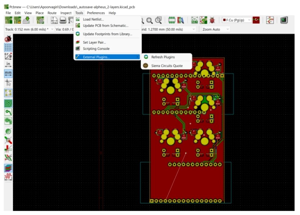
Decoding Common KiCad Headaches and How to Conquer Them
Let's dive into the most frequent stumbling blocks KiCad users encounter and, more importantly, how to systematically resolve them.
The Elusive Component: Tackling Library Errors
Picture this: you've meticulously drawn your schematic, only to find dreaded question marks or "Component Not Found" messages where your carefully chosen parts should be. This, my friend, is the quintessential library error, indicating that KiCad can't locate the symbolic representation (schematic library) or physical footprint (PCB library) for one or more of your components.
Why it Happens:
KiCad relies on libraries to define components. Each component has a schematic symbol (how it looks in the schematic editor) and a PCB footprint (how it looks on the board, including pad shapes and silkscreen). If the path to these library files is incorrect, or the library itself isn't added to your project's search paths, KiCad simply won't know what you're talking about. Common culprits include:
- Moving project files to a new location without updating paths.
- Sharing projects with others who have different library setups.
- Accidentally deleting a library or misnaming a path.
- Using custom libraries that aren't properly registered.
Resolution Steps:
- Verify Symbol Library Presence and Paths:
- Open your schematic.
- Navigate to
Preferences->Manage Symbol Libraries. - In the 'Project Specific Libraries' or 'Global Libraries' tab, scan the list. Are all the libraries you expect to use for this project listed?
- Crucially, check the 'Library Path' for each listed entry. Is it pointing to the correct
.kicad_symfile (or older.libfiles) on your system? Incorrect paths are a major source of frustration here.
- Add Missing Libraries:
- If a required library is entirely absent from the list, click the
Browse Librariesbutton (usually an icon that looks like a folder or a plus sign). - Navigate to where your KiCad libraries are stored (often in your KiCad installation directory or a custom location you've set up).
- Select the
.kicad_symfile for the missing library and click 'Open'. - Ensure you decide whether to add it as a 'Global Library' (available for all projects) or 'Project Specific Library' (only for the current project). For shared projects or specific needs, project-specific is often safer.
- Review and Correct Global Configuration Paths:
- If the issue persists, or you suspect a broader configuration problem, go to
Preferences->Configure Paths.... - Examine the listed environment variables, especially
KICAD_SYMBOL_DIRandKICAD_FOOTPRINT_DIR. These variables often point to your default KiCad library locations. Make sure they are pointing to valid directories on your system where KiCad's standard libraries reside. - Incorrect general path settings here can cascade into multiple library errors across projects.
Pro Tip: For project portability, always consider making copies of custom or essential third-party libraries and placing them within your project directory, then adding them as 'Project Specific Libraries'. This ensures that anyone opening your project has immediate access to the necessary components, regardless of their personal KiCad setup.
When Components Collide: Navigating PCB Designer Layout Issues
You've successfully transferred your netlist to the PCB editor, only to be greeted by a chaotic jumble of overlapping footprints, or worse, traces that refuse to connect properly despite your best efforts. These are classic PCB designer issues, encompassing everything from component placement to ensuring all electrical paths are properly formed.
Why it Happens:
The transition from a logical schematic to a physical PCB layout is where many design decisions become concrete. Overlapping components indicate poor spatial planning. Unconnected traces often stem from netlist discrepancies, incorrect pad-to-trace alignment, or even subtle layer misconfigurations. Mechanical layout issues might arise from neglecting physical constraints like enclosure size or connector positions.
Prevention is Your Best Defense:
Before you even think about laying out traces, dedicate significant time to component placement.
- Pre-Plan Your Layout in the Schematic: While the schematic is logical, having a rough physical layout in mind before you place components can save hours. Group related components, imagine the signal flow, and consider external connectors.
- Edit Component Placement Early: In the schematic editor, once components are placed, mentally group them into functional blocks. This early organization will translate much more smoothly to the PCB editor, minimizing the initial "rats' nest" of connections. Think about heat dissipation, signal integrity, and manufacturing assembly during this phase.
Resolution Steps for Overlapping Components: - Move and Arrange: Once in the PCB designer, if overlap has occurred, select the offending components (you can click and drag a box around them or select them individually).
- Utilize KiCad's Placement Tools:
- Use the
Mkey (Move) to drag components to new locations. - Use the
Rkey (Rotate) to orient them correctly. - For precise alignment, use the grid (hotkey
G) or theAlign/Distributetools found underToolsin the menu. - Consider the
Push and Shoverouter if you're working with existing traces – it will attempt to move traces aside to accommodate component movement.
Resolution Steps for Unconnected Traces (Open Circuits):
- Examine All Trace Connections on the PCB Editor: Visually inspect the "rats' nest" lines (representing connections from the netlist). If a trace doesn't automatically snap to a pad, or if a rats' nest line remains after you think you've routed a connection, there's a problem.
- Use the Trace Connection Tool (Route Tracks):
- Select the
Route Trackstool (often represented by a green line icon). - Click on a pad from which you want to start a trace. As you move the cursor, KiCad should highlight permissible pads/pins for that net. If it doesn't, or if it highlights the wrong pads, something is fundamentally wrong with your netlist or component association.
- Double-check that the component's footprint has the correct pin numbers associated with the schematic symbol's pin names. A common error is a mismatch here (e.g., schematic pin 1 connected to footprint pad 2).
- Ensure All Layers Are Selected When Making Connections (for Multi-Layer Boards):
- When routing a multi-layer board, you need to switch layers using the hotkeys (usually
+and-on the numeric keypad or the 'Active Layer' selector on the right toolbar). - If you're trying to connect a trace but can't reach the target, ensure you're on the correct layer, or that you're strategically placing vias to transition between layers.
- Visually confirm that the trace path is entirely on the intended layer(s) and that vias are properly placed to complete the connection between layers.
Pitfall to Avoid: Ignoring Design Rule Checker (DRC) warnings. KiCad's DRC (Tools->Design Rule Checker) is your best friend. It will flag clearance violations, unrouted nets, unplated holes too close to pads, and much more. Run it frequently during your layout process, not just at the end.
Size Matters: Fixing Scaling Issues for Production
You've spent hours perfecting your design, generating Gerber files for manufacturing, only to hear back from the fab house that your board dimensions are completely off. Scaling issues, particularly when exporting, are a common and frustrating problem.
Why it Happens:
Scaling problems typically arise from incorrect units (imperial vs. metric), export settings that don't match your design, or simply not explicitly defining the board's physical dimensions within KiCad. Modern PCB manufacturing is incredibly precise, and even a slight deviation in scale can render your board unusable.
Resolution:
- Ensure the PCB Design is at the Correct Scale:
- The first step is always to verify that your design within KiCad itself is dimensionally accurate. Use KiCad's measurement tools (
Measuretool, often represented by a ruler icon) to check critical distances and the overall board size. - Are you working in millimeters or inches? Be consistent. Most professional fab houses prefer millimeters. You can change units via
View->Switch UnitsorDimensions->Units.
- Check and Adjust Scaling Settings in PCB Size Settings:
- Navigate to
Dimensions->Page Settings(sometimes referred to asBoard Setupin newer versions, or similar). - Here, you'll find options to define your board's size and shape. Use the
Board Outlinetools (Draw a LineorAdd Graphic Line) on theEdge.Cutslayer to define your board's precise outer perimeter. - Crucially, when generating Gerber files (
File->Plot), review the 'Plot Options'. Ensure the 'Plot format' is set correctly (usually Gerber X2 or RS-274X) and that the 'Plot drill files' settings match your fab house's requirements (e.g., Excellon format, units, zero suppression). - There usually isn't an explicit "scaling factor" to adjust during Gerber export; rather, the problem is often that the dimensions of your board edge cuts aren't accurately defined, or the units in your project don't match the interpretation by the fab. Define your board dimensions precisely on the
Edge.Cutslayer.
Best Practice: Always send your fab house the latest version of yourEdge.Cutslayer, and ideally, a simple mechanical drawing with key dimensions to cross-reference. Many fab houses also provide specific KiCad export guidelines. Follow them precisely!
The Unbroken Path: Mastering Trace Connections
You've meticulously laid out your board, clicked "Route Tracks," and visually, everything looks connected. Yet, the Design Rule Checker still flags open circuits, or your fabricated board simply doesn't work. Incorrect connections are a subtle yet critical problem that can be tricky to debug.
Why it Happens:
An open circuit means there's a break in the electrical path you intended to create. This can happen if a trace doesn't quite touch a pad, if a via isn't correctly connected on both ends, or if a netlist mismatch prevents a proper connection from being recognized by KiCad's internal logic. Sometimes, it's a visual illusion – the trace looks connected, but mathematically, it isn't.
Resolution Steps:
- Check All Trace Connections on the PCB Editor (Visually and Logically):
- Visual Inspection: Zoom in significantly on any problematic areas, especially around pads and vias. Ensure traces fully overlap pad outlines and that vias are centered and connected to traces on all relevant layers.
- Highlight Net: Use the
Highlight Nettool (often a yellow highlight icon or hotkey~orV). Click on a pad or trace. KiCad will highlight all connected components and traces on that net. If parts of your circuit you expect to be highlighted are not, you've found an open circuit. - Netlist Comparison: If you suspect a deeper issue, regenerate your netlist from the schematic (
Tools->Generate Netlist) and then compare it against your PCB (Tools->Update PCB from Schematic). Look for discrepancies in net names or unrouted nets.
- Use the Trace Connection Tool (Route Tracks) to Correct Incorrect Paths:
- Instead of manually drawing lines that look like connections, always use the dedicated
Route Trackstool. This tool is "net-aware" – it understands which pads belong to which net and will only allow you to connect valid points. - If a connection is problematic, try deleting the trace segment (
Delete Tracktool) and re-routing it using theRoute Trackstool, letting KiCad's intelligence guide you. - Pay attention to the cursor feedback. It should snap to pads and highlight the current net.
- Ensure All Layers Are Selected When Making Connections (for Multi-Layer Boards):
- This is a common gotcha. If you're trying to route from one layer to another, you must explicitly place a via. Don't just draw a trace on one layer, then switch layers and expect it to magically connect.
- When routing, press the appropriate hotkey (e.g.,
Vor+on the keypad) to add a via and switch to the next layer. Continue routing on the new layer. - Visually confirm that the via is correctly connecting the traces on both layers. Use the layer visibility controls on the right-hand toolbar to isolate layers for inspection.
Multi-Layer Maze: Selecting and Configuring PCB Designer Layers
Multi-layer PCBs offer incredible design flexibility, allowing for dense layouts and improved signal integrity. However, managing these layers can be daunting, and incorrect configuration can lead to manufacturing errors or boards that simply don't function.
Why it Happens:
KiCad provides a robust layer stack-up manager, but if you don't correctly define the number of layers, their type (signal, power, ground, mixed), and their order, you'll run into issues. Common problems include traces being routed on internal non-signal layers, incorrect dielectric thicknesses, or missing copper planes.
Resolution Steps:
- Go to
Board Setup->Layers Setup:
- This is your central hub for configuring your PCB's layer stack-up.
- In the
Physical Stackuptab, you can define the total number of copper layers. KiCad defaults to 2, but you can increase it (4, 6, 8, etc.) as needed. - Crucially, assign
Layer Functions: For each internal layer, specify its role (e.g., 'Internal Plane' for solid ground/power planes, 'Internal Signal' for routing signal traces). This guides KiCad's routing behavior and ensures your Gerber outputs are correct. - Define the dielectric material and thickness between each layer. This is vital for impedance control and mechanical integrity; consult your chosen fab house's specifications.
- Select the Required Layers and Ensure All Relevant Layers Are Configured Correctly:
- Visibility Control: On the right-hand toolbar, you'll see a list of all available layers. Use the checkboxes to toggle their visibility. When routing, you'll actively switch between layers.
- Active Layer: Ensure you've selected the correct 'Active Layer' before drawing traces or placing vias. Routing on the wrong layer is a common mistake.
- Check
PlotSettings for Manufacturing: When generating Gerbers (File->Plot), make sure you select all the relevant layers for output. This includesF.Cu(Front Copper),B.Cu(Back Copper), and allIn(Internal Copper) layers, along with silkscreen, solder mask, and drill files. Forgetting to plot an internal copper layer is a guaranteed manufacturing fail.
Advanced Tip: For high-frequency designs or boards requiring precise impedance control, theLayers Setupdialog inBoard Setupallows you to define trace widths and spacings that meet specific impedance targets, often in conjunction with your fab house's material stack-up. Don't overlook these settings if your design demands it.
Beyond the Fix: Proactive Strategies for Flawless Designs
While knowing how to troubleshoot is essential, preventing problems in the first place is the hallmark of an experienced designer.
Prevention is Your Best Tool
Think of your design process as a series of checks and balances.
- Modular Design: Break complex designs into smaller, manageable schematic sheets. This makes debugging isolated issues much easier.
- Regular Netlist Updates: After significant changes in your schematic, always update the PCB from the schematic (
Tools->Update PCB from Schematic). Don't wait until the very end; frequent updates keep your schematic and layout synchronized. - Design Rule Checker (DRC): Run DRC early and often. It's not just for final verification; it's a powerful real-time design assistant that catches errors as you make them. Set up your DRC rules (
Board Setup->Design Rules) to match your manufacturer's capabilities before you start routing. - Electrical Rule Checker (ERC): Similar to DRC but for your schematic. The ERC (
Tools->Electrical Rule Checker) identifies common schematic errors like unconnected pins, conflicting outputs, or power supply issues. Run it frequently during schematic capture. - Version Control: Utilize a version control system (like Git) for your KiCad projects. This allows you to track changes, revert to previous versions if something goes wrong, and collaborate effectively.
The Power of Good Housekeeping: Backups and Resources
Even with the best preventative measures, unforeseen issues can crop up.
- Regular Backups: Make backing up your project a habit. KiCad can auto-save, but manually creating timestamped project archives (
File->Archive Project) before major changes, or at the end of a design session, is invaluable. A backup strategy can save you from corrupted files or accidental deletions. - Explore Available Tools and Resources:
- KiCad Documentation: The official KiCad documentation is comprehensive and constantly updated. It's often the fastest way to understand a specific feature or setting.
- Community Forums: The KiCad forum is an incredibly active and helpful resource. Chances are, if you've encountered a problem, someone else has too, and a solution is already documented.
- Online Tutorials and Videos: Numerous content creators offer excellent step-by-step guides for various KiCad functionalities.
By integrating these practices into your workflow, you'll not only become more adept at troubleshooting but also cultivate a more robust and reliable design process.
KiCad Troubleshooting FAQs: Quick Answers to Common Queries
Why is my KiCad component missing even after I've placed it in the schematic?
This is almost certainly a library error. KiCad cannot find the schematic symbol or PCB footprint for that component in its configured library paths. Revisit Preferences -> Manage Symbol Libraries and Manage Footprint Libraries to ensure the correct library is listed and its path is accurate. If you've just created a custom part, ensure you saved it to a registered library and updated your project.
How do I avoid common layout mistakes like component overlaps or misaligned traces in KiCad?
The best defense is proactive planning. Spend significant time on initial component placement in the PCB editor, thinking about signal flow, mechanical constraints, and thermal considerations. Group related components, space them adequately, and try to visualize trace paths before you start routing. Use the Move and Rotate tools extensively. Always run the Design Rule Checker (DRC) frequently – it will highlight overlaps and clearance violations instantly.
Can I recover a corrupted KiCad project?
Sometimes, yes. Regular backups are your first line of defense. KiCad often creates .kicad_pcb-bak and .kicad_sch-bak files (backup files) in your project directory; you can rename these by removing the -bak extension to revert to a previous state. If you use version control (like Git), you can easily revert to an earlier, stable commit. For severe corruption, a clean install of KiCad and restoring from a recent backup might be necessary.
My traces look connected, but DRC says "Unconnected Items." What gives?
This typically means the trace isn't mathematically connected to the pad or via, even if it appears to touch it visually. Zoom in extremely close on the problematic areas. Often, the trace is just a pixel or two off. Delete the offending trace segment and re-route it using the Route Tracks tool, letting KiCad's snap-to-grid and net-aware features ensure a proper connection. Also, make sure the component's footprint has correctly defined pads with the right net associations.
How do I ensure my board's dimensions are accurate for the manufacturer?
Define your board's outline precisely using graphic lines on the Edge.Cuts layer in the PCB editor. Go to Dimensions -> Page Settings (or Board Setup) to define the overall board size and ensure your units are consistent (usually millimeters). When generating Gerber files (File -> Plot), double-check the plot settings to ensure no unintended scaling or unit conversions occur, and always send a copy of your Edge.Cuts layer and ideally a dimensioned drawing to your fab house for verification.
Your Journey to KiCad Mastery
Troubleshooting KiCad isn't about magical fixes; it's about understanding the software's logic and approaching problems systematically. Every error message, every misaligned trace, and every "component not found" is a learning opportunity. By embracing the preventative measures, meticulously checking your settings, and leveraging KiCad's powerful built-in tools, you'll not only resolve current issues faster but also build a robust design workflow that minimizes future headaches.
Remember, the goal isn't just to fix the problem, but to understand its root cause. With each hurdle you conquer, your expertise grows, transforming you from a frustrated user into a confident KiCad master, ready to bring your most ambitious electronic designs to life. Keep designing, keep learning, and keep creating.